供应德州仪器的高速模数转换器集成电路ADS62C17IRGCT
| 价 格: | 390.00 | |
| 型号/规格: | ADS62C17IRGCT /VQFN(RGC)/64 | |
| 品牌/商标: | TI (Texas Instruments德州仪器) |
TI 主页 > 半导体 > 数据转换器 > 模数转换器 > 高速 ADC (>10MSPS) > adss62c17irgct
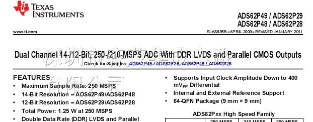
具有 SNRBoost 的双通道 11 位 200MSPS ADC 集成电路 ADS62C17IRGCT
Dual Channel 11 Bit, 200 MSPS ADC with SNRBoost ADS62C17IRGCT
数据列表 ADS62C17
产品相片 64-VQFN_ExposedPad
标准包装 250
类别 集成电路 (IC)
家庭 数据采集 - 模数转换器
系列 -
位数 11
采样率(每秒) 200M
数据接口 串行, 并联
转换器数目 2
功率耗散() 1.1W
电压电源 模拟和数字
工作温度 -40°C ~ 85°C
安装类型 表面贴装
封装/外壳 64-VFQFN 裸露焊盘
供应商设备封装 64-VQFN 裸露焊盘 (9x9)
包装 带卷 (TR)
输入数目和类型 2 个差分,单极
说明
ADS62C17 is a dual channel 11-bit, 200 MSPS A/D converter that combines high dynamic performance and low power consumption in a compact 64 QFN package. This makes it well-suited for multi-carrier, wide band-width communications applications.
ADS62C17 uses TI-proprietary SNRBoost technology that can be used to overcome SNR limitation due to quantization noise for bandwidths less than Nyquist (Fs/2). It includes several useful and commonly used digital functions such as ADC offset correction, gain (0 to 6 dB in steps of 0.5 dB) and gain tuning (in fine steps of 0.001 dB).
The gain option can be used to improve SFDR performance at lower full-scale input ranges. Using the gain tuning capability, each channel’s gain can be set independently to improve channel-to-channel gain matching.
ADS62C17是一个双通道11位,200 MSPS A / D转换,结合在一个紧凑的64 QFN封装的高动态性能和低功耗。这使得它非常适合多载波,宽带宽通信应用。
ADS62C17采用TI专有的SNRBoost技术可用于克服信噪比由于量化噪声的带宽小于奈奎斯特(FS / 2)的限制。它包括几个有用的和常用的数码功能,如ADC的偏移校正,增益(0至6分贝步长为0.5分贝)和增益调整(精度0.001分贝)。
增益选项,可用于改善在较低的满量程输入范围的SFDR性能。使用增益调整功能,每个通道的增益可以独立设置,以提高通道对通道增益匹配。
View full Description in Datasheet
特性
Maximum Sample Rate: 200 MSPS
11-bit Resolution with No Missing Codes
90 dBc SFDR at Fin = 10 MHz
79.8 dBFS SNR at 125 MHz IF, 20 MHz BW
using TI proprietary SNRBoost technology
Total Power 1.1 W at 200 MSPS
90 dB Cross-talk
Double Data Rate (DDR) LVDS and Parallel
CMOS Output Options
Programmable Gain up to 6dB for SNR/SFDR Trade-off
DC Offset Correction
Gain Tuning Capability in Fine Steps (0.001 dB)
Allows Channel-to-channel Gain Matching
Supports Input Clock Amplitude Down to
400 mV p-p Differential
Internal and External Reference Support
64-QFN Package (9 mm × 9 mm)
参数
ADS62C15 ADS62C17
Resolution(Bits) 11 11
Sample Rate (max) 125MSPS 200MSPS
# Input Channels 2 2
Interface LVDS, Parallel and Serial SPI Interface LVDS, Parallel and Serial SPI Interface
SNR(dB) 67.2 67
SFDR(dB) 89 85
Power Consumption(Typ)(mW) 740 1081
Operating Temperature Range(°C) -40 to 85 -40 to 85
Rating Catalog Catalog
Analog Voltage AV/DD(Min)(V) 3 3.15
Analog Voltage AV/DD(Max)(V) 3.6 3.8
Digital Supply(Min)(V) 3 1.7
Digital Supply(Max)(V) 3.6 1.9
Architecture Pipeline Pipeline
INL(Max)(+/-LSB) 3.5 2.5
SINAD(dB) 67.1 66.9
ENOB(Bits) 10.8 10.8
Input Range 2V (p-p) 2V (p-p)
Reference Mode Int and Ext Int and Ext
供应TI 的立体声音频音量控制集成电路PGA2310pa.ua
信息内容:TI 主页 > 半导体 > 音频 > 音量控制 > pga2310pa.pga2310ua 德州仪器的 +/-15V 立体声音频音量控制集成电路PGA2310PA PGA2310UA PGA2310: Stereo Audio Volume Control PGA2310依据封装不同,可以分为 PGA2310PA PGA2310UA 说明 The PGA2310 is a high-performance, stereo audio volume control designed for professional and high-end consumer audio systems. The ability to operate from ±15V analog power supplies enables the PGA2310 to process input signals with large voltage swings, thereby preserving the dynamic range available in the overall signal path. Using high performance operational amplifier stages internal to the PGA2310 yields low noise and distortion, while providing the capability to drive 600 loads directly without buffering. The three–wire serial control interface allows for connection to a wide variety of host controllers. In addition to support for daisy–chaining of multiple PGA2310 devices. 特性 DIGITALLY–CONTROLLED ANALOG VOLUME CONTROL Two Indep...
供应TI 的高速14位模数转换器集成电路ADS62P48IRGCT
信息内容:TI > 半导体 > 数据转换器 > 模数转换器 > 高速 ADC (>10MSPS) >集成电路ADS62P48IRGCT 具有 DDR LVDS 和并行 CMOS 输出的双通道 14 位、210MSPS ADC Dual Channel 14-/12-Bit, 250/210 MSPS ADC with DDR LVDS & Parallel CMOS Outputs 说明 The ADS62Px9/x8 is a family of dual channel 14-bit and 12-bit A/D converters with sampling rates up to 250 MSPS. It combines high dynamic performance and low power consumption in a compact 64 QFN package. This makes it well-suited for multi-carrier, wide band-width communications applications. The ADS62Px9/x8 has gain options that can be used to improve SFDR performance at lower full-scale input ranges. It includes a dc offset correction loop that can be used to cancel the ADC offset. Both DDR LVDS (Double Data Rate) and parallel CMOS digital output interfaces are available. It includes internal references while the traditional reference pins and associated decoupling capacitors have been eliminated. View full Description in Datasheet 特性...


