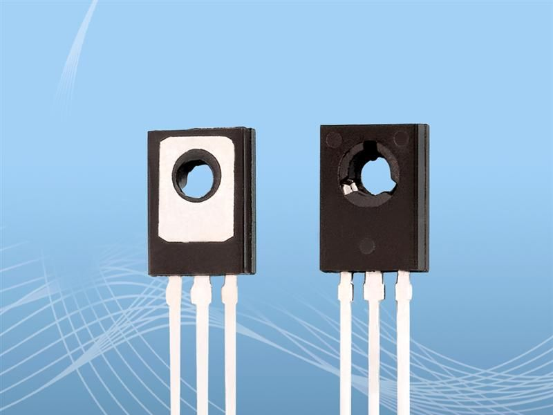
三极管G13002/G13003
| 价 格: | 面议 | |
| 型号/规格: | G13002/G13003 | |
| 品牌/商标: | SZGKT | |
| 封装形式: | TO-220 | |
| 环保类别: | 无铅环保型 | |
| 安装方式: | 直插式 | |
| 包装方式: | 单件包装 |
DESCRIPTION:
These devices are designed for high–voltage, high–speed power switching inductive
circuits where fall time is critical. They are particularly suited for 115 and 220 V SWI-
TCHMODE applications such as Switching Regulators, Inverters, Motor Controls, Sol-
enoid/Relay drivers and Deflection circuits.
FEATURES:
* Reverse Biased SOA with Inductive Loads @ TC = 100℃
* Inductive Switching Matrix 0.5 to 1.5 Amp,
25 and 100℃. . . tc @ 1 A, 100℃ is 290 ns (Typ).
* 700 V Blocking Capability
* SOA and Switching Applications
Information
MAXIMUM RATINGS:
Symbol
Rating
G13002
G13003
Unit
VCEO(sus)
Collector–Emitter Voltage
300
400
Vdc
VCEV
Collector–Emitter Voltage
600
700
Vdc
VEBO
Emitter Base Voltage
9
Vdc
IC
Collector Current —
Continuous
1.5
Adc
ICM
— Peak (1)
3
IB
Base Current — Continuous
0.75
Adc
IBM
— Peak (1)
1.5
IE
Emitter Current — Continuous
2.25
Adc
IEM
— Peak (1)
4.5
Tj , Tstg
Operating and
StorageJunctionTemperatureRange
–65 to +150
℃
ELECTRICAL
CHARACTERISTICS: (TC = 25℃ unless otherwise
noted)
SYMBOL
CHARACTERISTICS
MIN
TYP
MAX
UNIT
ICEV
VCEV = Rated Value, VBE(off) = 1.5
Vdc
1
mAdc
VCEV = Rated Value, VBE(off) = 1.5 Vdc,
TC = 100 .
5
IEBO
(VEB = 9 Vdc, IC = 0)
1
mAdc
hFE
IC = 0.5 Adc, VCE = 2 Vdc
8
40
IC = 1 Adc, VCE = 2 Vdc
5
25
VCE(sat)
(IC = 0.5 Adc, IB = 0.1 Adc)
0.5
Vdc
(IC = 1 Adc, IB = 0.25 Adc)
1
(IC = 1.5 Adc, IB = 0.5 Adc)
3
(IC = 1 Adc, IB = 0.25 Adc, TC =
100 .)
1
VBE(sat)
IC = 0.5 Adc, IB = 0.1 Adc)
1
Vdc
(IC = 1 Adc, IB = 0.25 Adc)
1.2
(IC = 1 Adc, IB = 0.25 Adc, TC =
100 . )
1.1
fT
(IC = 100 mAdc, VCE = 10 Vdc, f = 1
MHz)
4
10
MHz
td
(VCC = 125 Vdc, IC = 1 A,
IB1 = IB2 = 0.2 A, tp = 25 ms,
Duty Cycle _ 1%)
0.05
0.1
us
tr
0.5
0.1
us
ts
2
4
us
tf
0.4
0.7
us
- 所属城市:广东 深圳
- [联系时请说明来自维库仪器仪表网]
- 联系人: 翁经理/许小姐/谢小姐
- 电话:0755-27578409/27578368
- 传真:0755-27578290
- 手机:15999672043/13823390688/15019404824
- QQ :


三极管L7812
信息内容:Electrical Characteristics Of L7812 (refer to the test circuits, TJ = -55 to 150°C, VI = 19V, IO = 500 mA, CI = 0.33 μF, CO = 0.1 μF unless otherwise specified). Symbol Parameter Test Conditions Min Typ Max Unit VO Output Voltage TJ= 25°C 11.5 12 12.5 V VO Output Voltage IO = 5 mA to 1 A, PO ≤ 15W VI = 15.5 to 27 V 11.4 12 12.6 V ...

三极管 B772
信息内容:FEATURES: * Power dissipation: Pcm : 500 mW * Collector current: Icm : -3 A * Collector-base voltage: V(BR)CBO : -40 V * Operating and storage junction temperature range : Tj, Tstg : -55℃ to +150℃ ELECTRICAL CHARACTERISTICS: Symbol Test conditions MIN TYP MAX Unit V(BR)CBO Ic=-100uA, IE=0 -40 V V(BR)CEO IC= -10mA, IB=0 -30 ...


