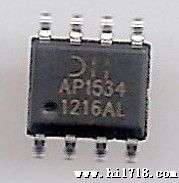
&sp;AP1534
PWM CONTROL 2A STEP-DOWN CONVERTER
AP1534 Rev. 2 1 of 8 DECEER 2007
www.diod.com© Diod Incorporated
• Input voltage: 4.4V to 18V
• Output voltage: 0.8V to VCC.
• Duty ratio: 0% to 99% PWM control
• Oscillation frequency: 300KHz t.
• Current limit, Enable funion
• Thermal Shutdown funion
• Built-in internal SW P-channel MOS
• SOP-8L: ailable in “Green” Molding Compound
( Br, Sb)
• Lead Free Finish/RoHS Compliant (te 1)
AP1534 consists of step-down switching regulator with PWM
control. The devic include a reference voltage source,
oscillation circuit, error amplifier, internal PMOS.
AP1534 provid low-ripple power, high efficiency, and excellent
transient charaeristics. The PWM control circuit is able to vary
the duty ratio linearly from 0 up to 99%. This converter also
contains an error amplifier circuit as well as a soft-start circuit that
prevents overshoot at startup. An enable funion, an over
current prote funion and a short circuit prote funion are built
inside, and when OCP or SCP happens, the operation frequency
will be reduced from 300KHz to 50KHz. Also, an internal
compensation block is built in to minimize external component
count.
With the addition of an internal P-channel Power MOS, a coil,
capacitors, and a diode conneed externally, the ICs can
funion as step-down switching regulators. They serve as ideal
power supply units for portable devic when coupled with the
SOP-8L mini-packag, providing such outstanding featur as
low current consumption. Since this converter can accommodate
an input voltage up to 18V, it is also suitable for the operation via
an AC adapter.
• PC Motherboard
• LCD Monitor
• Graphic Card
• DVD-Video Player
• Telecom Equipment
• ADSL Modem
• Printer and other Peripheral Equipment
• Microprocsor Core Supply
A P 1 5 3 4 X X X
Package Packing
S : SOP-8L
Lead Free
-U : Tube
-13 : Tape & Reel
G : Green
te: 1. RoHS revision 13.2.2003. Gl and High Temperature Solder Exemptions Applied, see EU Direive Annex t 5 and 7.
Tube 13” Tape and Reel
Device Package
Code
Packaging
(te 2) Quantity Part Nuer
Suffix
Quantity Part Nuer
Suffix
AP1534S S SOP-8L 100 -U 2500/Tape & Reel -13
te: 2. Pad layout as shown on Diod Inc. suggted pad layout document AP02001, which can be found on our website at
https://www.diod.com/datasheets/ap02001.pdf.
Featur General Dcription
Applications
Ordering Information
AP1534
PWM CONTROL 2A STEP-DOWN CONVERTER
AP1534 Rev. 2 2 of 8 DECEER 2007
www.diod.com© Diod Incorporated
Pin ignments
1
2
3
4
8
7
6
5
FB
OCSET Output
Output
EN
Vss
Vss
VCC
SOP-8L
AP1534
Pin Dcriptions
Pin Name Pin . Dcription
FB 1 Feedback pin
EN 2
Power-off pin
H: rmal operation
(Step-down operation)
L: Step-down operation sped
(All circuits deaivated)
OCSET 3 Add an external ristor to set max output current
VCC 4 IC power supply pin
Output 5, 6 Switch Pin. Conne external induor/diode here. Minimize
trace area at this pin to reduce EMI
VSS 7, 8 GND Pin
AP1534
PWM CONTROL 2A STEP-DOWN CONVERTER
AP1534 Rev. 2 3 of 8 DECEER 2007
www.diod.com© Diod Incorporated
Block Diagram
Oscillation
Circuit
Reference Voltage
Source
PWM-Switched
Control Circuit
+
-
V Vss EN
EN
100uA
OCSET
FB
Vcc
Thermal
Shutdown
Output
Absolute Maximum Ratings
Syol Parameter Rating Unit
D HBM Human Body Model D Proteion 4.5 KV
D MM Machine Model D Proteion 150 V
VCC VCC Pin Voltage VSS - 0.3 to VSS + 20 V
VFB Feedback Pin Voltage VSS - 0.3 to VCC V
VEN EN Pin Voltage VSS - 0.3 to VIN V
VOUT Switch Pin Voltage VSS - 0.3 to VIN V
PD Power Dissipation Internally limited mW
TJ Operating Junion Temperature Range -20 to +125 oC
TST Storage Temperature Range -40 to +150 oC
Caution: The absolute maximum ratings are rated valu exceeding which the produ could suffer physical damage.
The valu must therefore t be exceeded under any conditions.
Recommended Operating Conditions
Syol Parameter Min Max Unit
VIN Input Voltage 4.4 18 V
IOUT Output Current 0 2 A
TA Operating Aient Temperature -25 85 oC
AP1534
PWM CONTROL 2A STEP-DOWN CONVERTER
AP1534 Rev. 2 4 of 8 DECEER 2007
www.diod.com© Diod Incorporated
Elerical Charaeristics ( VIN = 12V, TA = 25°C, unls otherwise specified )
Syol Parameter Conditions Min T. Max Unit
VFB Feedback Voltage IOUT = 0.1A 0.784 0.8 0.816 V
IFB Feedback Bias Current IOUT = 0.1A - 0.1 0.5 μA
ISW Switch Current -- 2.0 - - A
ISHDN Current Consumption
During Power Off VEN = 0V - 10 - μA
ΔVOUT
/ VIN Line Regulation VIN = 5V~18V - 1 2 %
ΔVOUT
/VOUT Load Regulation IOUT = 0.1 to 2A - 0.2 0.5 %
fOSC Oscillation Frequency Measure weform at SW pin00 KHz
fOSC1 Frequency of Current Limit
or Short Circuit Prote Measure weform at SW pin - 50 - KHz
VIH Evaluate oscillation at SW pin 2.0 - -
VIL EN Pin Input Voltage Evaluate oscillation s at SW pin - - 0.8 V
ISH -- - 20 - μA
ISL
EN Pin Input Leakage
Current -- - -10 - μA
IOCSET OCSET Pin Bias Current μA
RDS(ON) Internal MOSFET RDS(ON) VVIINN == 152VV, V, VFBF B= = 0 V0V -- 116000 -- mΩ
EFFI Efficiency VIN = 12V, VOUT = 5V
IOUT = 2A - 91 - %
TSHDN Thermal shutdown thrhold - 150 - °C
THYS Thermal shutdown
hysteris - 55 - °C
θJA Thermal Ristance
Junion-to-Aient SOP-8L (te 3) - 127 - oC/W
θJC Thermal Ristance
Junion-to-Case SOP-8L (te 3) - 28 - oC/W
te: 3. Tt condition for SOP-8L: Device mounted on FR-4 substrate PC board, 2oz copper, with minimum recommended pad layout.
For better thermal performance, larger copper pad for heatsink is needed.
Tical Application Circuit
AP1534
+
V - EN SS
CC
RA
B240A RB
FB
Vcc Output
CVcc
VOUT =5V/2A
VIN
ROCSET
OCSET COUT CIN
Optional
COCSET
CEN
REN
Option
100K
te: VOUT = VFB x (1+RA /RB)
RB =0.7K~5K ohm
L1
22uH
6.8K
1.3K
5.6K
0.1uF
+
-
C
470uF 0.1uF 470uF
0.1uF (te 4)
D1
te: 4. Suggted DIOD Power Schottky P/N: B240/B340 seri.
AP1534
PWM CONTROL 2A STEP-DOWN CONVERTER
AP1534 Rev. 2 5 of 8 DECEER 2007
www.diod.com© Diod Incorporated
Tical Performance Charaeristics
VIN vs Frequency
(VOUT=3.3V, IOUT=0.2A)
306
308
310
312
314
316
318
320
322
324
326
0 2 4 6 8 1 18
VIN (V)
FOSC (kHz)
VIN vs VFB
(VOUT=3.3V, IOUT=0.2A)
0.780
0.785
0.790
0.795
0.800
0.805
0.810
0.815
0.820
0 2 4 6 8 1 18
VIN (V)
VFB (V)
Line Regulation
(VOUT=3.3V, IOUT=0.2A)
-3.0%
-2.0%
-1.0%
0.0%
1.0%
2.0%
3.0%
0 2 4 6 8 1 18
VIN (V)
VOUT CHANGE (%)
Load Regulation
(VIN=5V, VOUT=3.3V)
-1.0%
-0.8%
-0.6%
-0.4%
-0.2%
0.0%
0.2%
0.4%
0.6%
0.8%
1.0%
0.0 0.5 IO1UT.0 (A) 1.5 2.0
VOUT CHANGE (%) Efficiency
0
10
20
30
40
50
60
70
80
90
100
0.0 0.5 1.0 1.5 2.0
IOUT (A)
Efficiency (%)
VOUT=3.3V
VOUT=5V
AP1534
PWM CONTROL 2A STEP-DOWN CONVERTER
AP1534 Rev. 2 6 of 8 DECEER 2007
www.diod.com© Diod Incorporated
Tical Performance Charaeristics (Continued)
Vout Ripple
(Vin=5V, Vout=3.3V, Iout=0.1A)
Vout Ripple
(Vin=5V, Vout=3.3V, Iout=2A)
Tt Circuit
A
VCC FB
VSS
EN
open
open
FB
EN
+
-
Oscillation
OUTPUT A OUTPUT
FB
EN
+
-
+
-
V
OUTPUT
OCSET
OCSET
OCSET
Enable funion tt Feedback funion tt
Operation funion tt
VCC
VCC
VSS
VSS
AP1534
PWM CONTROL 2A STEP-DOWN CONVERTER
AP1534 Rev. 2 7 of 8 DECEER 2007
www.diod.com© Diod Incorporated
Funion Dcription
PWM Control
The AP1534 is a DC/DC converter that employs pulse width
modulation (PWM) scheme. Its pulse width vari in the range of
0% to 99%, based on the output current loading. The output
ripple voltage caused by the PWM high frequency switching can
easily be reduced through an output filter. Therefore, this
converter provid a low ripple output supply over a broad range
of input voltage & output current loading
Under Voltage Lockout
The under voltage lockout circuit of the AP1534 ur that the
high-side MOSFET driver remains in the off state whe the
supply voltage drops below 3.3V. rmal operation rum
once VCC ris above 3.5V.
Current Limit Proteion
The current limit thrhold is set by external ristor ROCSET
conneed from VCC supply to OCSET pin. The internal sink
current IOCSET (90uA tical) across this ristor sets the voltage
at OCSET pin. When the PWM voltage is ls than the voltage at
OCSET, an over-current condition is triggered.
The current limit thrhold is given by the following equation:
IPEAK RDS(ON) IOCSET ROCSET
&tim; = &tim;
2
( I)
IPEAK IOUT (MAX)
Δ
> +
where,
IN
OUT
S
IN OUT
V
V
x
F xL
V V
I
−
Δ =
IPEAK is the output peak current; RDS (ON) is the MOSFET ON
ristance; FS is the PWM frequency (300KHz tical). Also, the
induor value will affe the ripple current ΔI.
The above equation is recommended for input voltage range of
5V to 18V. For input voltage lower than 5V, higher than 18V or
aient temperature over 100°C, ROCSET≧6.8KΩ is
recommended.
The recommended minimum ROCSET value is summarized below:
VIN (V) VOUT (V) ROCSET (Ω)
4 1 6.8K
5 3.3 5.6K
12 5 3.9K
18 12 4.7K
The maximum ROCSET value should t exceed AP1533 maximum
current output.
( View )
SOP-8L
AP1534
WWX X
Logo
Part .
Internal code
Year : "07" = 2007
"08" = 2008
Xth week: 01~52
~
8 5
1 4
G : Green
Marking Information
AP1534
PWM CONTROL 2A STEP-DOWN CONVERTER
AP1534 Rev. 2 8 of 8 DECEER 2007
www.diod.com© Diod Incorporated
Package Information (All Dimensions in mm)
1.27t 0.3/0.5
7°~9°
4.80/5.30
3.70/4.10
5.79/6.20
0.20t
7°~9°
3.70/4.10
0.38/1.27
0.08/0.25
Gauge Plane
0.254
Seating Plane
0.35max.45°
Detail "A"
Detail "A"
1.30/1.50
1.75max.
Land Pattern Recommendation
0.78
(Unit: mm)
6x-1.27
8x-1.55
8x-0.60
5.4
IMPORTANT TICE
LIFE SUPPORT
Diod Incorporated and its subsidiari rerve the right to make modifications, enhancements, improvements, correions or other chang without further
tice to any produ herein. Diod Incorporated do t ume any liability arising out of the application or use of any produ dcribed herein; neither
do it convey any license under its patent rights, r the rights of others. The user of produs in such applications shall ume all risks of such use and will
agree to hold Diod Incorporated and all the compani whose produs are reprented on our website, harmls against all damag.
Diod Incorporated produs are t authorized for use as critical components in life support devic or systems without the exprsed written approval of the
Prident of Diod Incorporated.
联系电话:0755—&sp;传真:0755—
联系人:廖小姐&sp;&sp;&sp;郭先生


