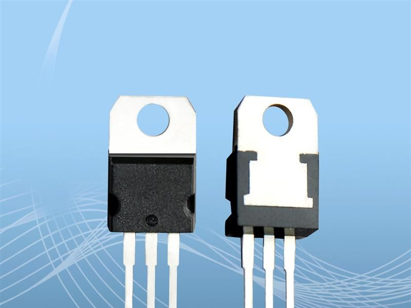
三极管L7800 series
| 价 格: | 面议 | |
| 型号/规格: | L7800 series | |
| 品牌/商标: | SZGKT | |
| 封装形式: | TO-220 | |
| 环保类别: | 无铅环保型 | |
| 安装方式: | 直插式 | |
| 包装方式: | 单件包装 |
FEATURES:
* OUTPUT CURRENT TO
1.5A
* OUTPUT VOLTAGES OF 5; 5.2; 6; 8; 8.5;
9;10; 12; 15; 18;
24V
* THERMAL OVERLOAD PROTECTION
* SHORT CIRCUIT PROTECTION
* OUTPUT TRANSITION SOA
PROTECTION
DESCRIPTION:
The L7800 series of three-terminal positive regulators is available in TO-220, TO-220FP,TO-220FM,
TO-3 and D2PAK packages and several fixed output voltages, making it useful in a wide range of
applications. These regulators can provide local on-card regulation, eliminating the distribution
problems associated with single point regulation. Each type employs internal currentlimiting, thermal
shut-down and safe area protection, making it essentially indestructible. If adequate heat sinking is
provided, they can deliver over 1A output current. Although designed primarily as fixed voltage reg-
ulators, these devices can be used with external components to obtain adjustable voltage and currents.
ABSOLUTE MAXIMUM RATINGS:
|
Symbol |
Parameter |
Value |
Unit |
||
|
VI |
DC Input Voltage |
for VO= 5 to 18V |
35 |
V |
|
|
for VO= 20, 24V |
40 |
||||
|
IO |
Output Current |
Internally Limited |
|
||
|
Ptot |
Power Dissipation |
Internally Limited |
|
||
|
Tstg |
Storage TemperatureRange |
-65 to 150 |
°C |
||
|
Top |
Operating Junction Temperature Range |
for L7800 |
-55 to 150 |
°C |
|
|
for L7800C |
0 to 150 |
||||
Electrical
Characteristics Of L7805 (refer to the test circuits, TJ = -55 to
150°C, VI = 10V,
IO =
500 mA, CI = 0.33 μF, CO = 0.1 μF unless otherwise specified).
|
Symbol |
Parameter |
Test Conditions |
Min |
Typ |
Max |
Unit |
|
VO |
Output Voltage |
TJ= 25°C |
4.8 |
5 |
5.2 |
V |
|
VO |
Output Voltage |
IO = 5 mA to 1 A, PO ≤ 15W VI = 8 to 20 V |
4.65 |
5 |
5.35 |
V |
|
△VO |
Line Regulation |
VI = 7 to 25 V, TJ = 25°C |
|
3 |
50 |
mV |
|
VI = 8 to 12 V, TJ = 25°C |
|
1 |
25 |
|||
|
△VO |
Load Regulation |
IO=5 mA to 1.5 A, TJ = 25°C |
|
|
100 |
mV |
|
IO=250 to 750 mA,TJ = 25°C |
|
|
25 |
|||
|
ID |
Quiescent Current |
TJ= 25°C |
|
|
6 |
mA |
|
△ID |
Quiescent Current Change |
IO = 5 mA to 1 A |
|
|
0.5 |
mA |
|
VI = 8 to 25 V |
|
|
0.8 |
|||
|
eN |
Output Noise Voltage |
B =10Hz to 100KHz TJ = 25°C |
|
|
40 |
uV/VO |
|
SVR |
Supply Voltage Rejection |
VI = 8 to 18 V, f = 120Hz |
68 |
|
|
dB |
|
VD |
Dropout Voltage |
IO = 1 A,TJ = 25°C |
|
2 |
2.5 |
V |
|
RO |
Output Resistance |
f = 1 KHz |
|
17 |
|
mΩ |
|
Isc |
Short Circuit Current |
VI = 35 V, TJ = 25°C |
|
0.75 |
1.2 |
A |
|
Iscp |
Short CircuitPeak Current |
TJ = 25°C |
1.3 |
2.2 |
3.3 |
A |
- 所属城市:广东 深圳
- [联系时请说明来自维库仪器仪表网]
- 联系人: 翁经理/许小姐/谢小姐
- 电话:0755-27578409/27578368
- 传真:0755-27578290
- 手机:15999672043/13823390688/15019404824
- QQ :


三极管8550
信息内容:GENERAL DESCRIPTION: The 8550 is a PNP epitaxial silicon planer transistor designed for use in the audio output stage and converter/inverter circuits. Complementary to 8050. ABSOLUTE MAXIMUM RATINGS: Symbol Parameter Value Units VCBO Collector-Base Voltage 30 V VCEO Collector-Emitter Voltage 25 V VEBO Emitter-Base Voltage 6 V Ic ...


