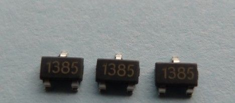
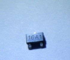
Low Power Hall Switch YH4915
GENERAL DESCRIPTION
The YH4915 omnipolar Hall effect sensor IC is fabricated from mixed signal CMOS
technology .It ncorporates advanced chopper-stabilization techniques to provide accurate
and stable magnetic switch points.
The circuit design provides an internally controlled clocking mechanism to cycle
power to the Hall element and analog signal processing circuits. This serves to place
the high current-consuming portions of the circuit into a “Sleep” mode. Periodically the
device is “Awakened” by this internal logic and the magnetic flux from the Hall element
is evaluated against the predefined thresholds. If the flux density is above or below the
Bop/Brp thresholds then the output transistor is driven to change states accordingly.
While in the “Sleep” cycle the output transistor is latched in its previous state. The
design has been optimized for service in applications requiring extended operating
The output transis or of the YH4915 will be latched on (Bop) in the presence
of a sufficiently strong South or North magnetic field facing the marked side of the
package. The output will be latched off (Brp) in the absence of a magnetic field.
Features
2.4V-5.5V battery operation
High sensitivity and high stability of the magnetic switching
High resistance to mechanical stress
Digital output signal
Switching for both poles of a magnet (omnipolar)
- 所属城市:广东 深圳
- [联系时请说明来自维库仪器仪表网]
- 联系人: 陈愈柏
- 电话:0755-84664302/84660586-618
- 传真:0755-84662603
- 手机:18923809726
- QQ :
供应高灵敏度全极性微功耗霍尔开关YH4915
信息内容:Low Power Hall Switch YH4915 GENERAL DESCRIPTION The YH4915 omnipolar Hall effect sensor IC is fabricated from mixed signal CMOS technology .It ncorporates advanced chopper-stabilization techniques to provide accurate and stable magnetic switch points. The circuit design provides an internally controlled clocking mechanism to cycle power to the Hall element and analog signal processing circuits. This serves to place the high current-consuming portions of the circuit into a “Sleep” mode. Periodically the device is “Awakened” by this internal logic and the magnetic flux from the Hall element is evaluated against the predefined thresholds. If the flux density is above or below the Bop/Brp thresholds then the output transistor is driven to change states accordingly. While in the “Sleep” cycle the output transistor is latched in its previous state. The design has been optimized for service in applications r...
供应全极性微功耗霍尔开关YH4916
信息内容:深圳市裕辉美科技有限公司YH4916 CMOS输出无极性高灵敏度微功耗霍尔开关 产品概述 YH4916是一款基于混合信号CMOS技术的无极性霍尔开关,这款IC采用了先进的斩波稳定技术,因而能够提供准确而稳定的磁开关点。 在电路设计上,YH4916提供了一个内嵌的受控时钟机制来为霍尔器件和模拟信号处理电路提供时钟源,同时这个受控时钟机制可以发出控制信号使得消耗电流较大的电路周期性的进入“休眠”模式;同样通过这个机制,芯片被周期性的“唤醒”并且根据预定好的磁场强度阈值检测外界穿过霍尔器件磁场强度的大小。如果磁通密度高于“操作点”阈 值或者低于“释放点”阈值,则CMOS输出被驱动并锁存成与之相对应的状态。而在“休眠”周期中,输出晶体管被锁定在其先前的状态下。在电池供电应用中,这种设计对于延长工作寿命提供了支持。 YH4916的CMOS输出在面向封装标示一面存在一定强南极或北极磁场时被锁定在输出高状态,而在无磁场时锁定在低状态。 额定工作参数 工作温度范围 TMIN ≤ TA ≤ TMAX −40°C ≤ TA ≤ 85°C 工作电压范围 2.4V ≤ VDD ≤ 5.5V 产品特点 2.4V — 5.5V电...


