mosfet应用, 中低压场效应管mosfet应用|多项技术
| 价 格: | 面议 | |
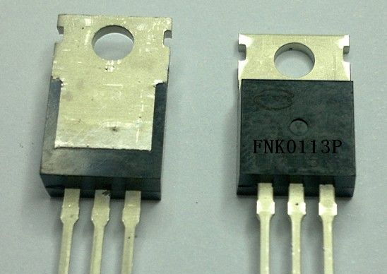
| 型号/规格: | FNK0113P | |
| 品牌/商标: | FNK | |
| 封装形式: | TO-220 | |
| 环保类别: | 无铅环保型 | |
| 安装方式: | 直插式 | |
| 包装方式: | 卷带编带包装 |
乾野电子在目前(20V-250V)大功率Trench-MOS 器件、(500V-650V)SJ-MOS器件、普通高压MOS器件(600V)已量产与销售, 并取得国内和国际的多项技术。
MOSFET的参数介绍
|
Parameter |
Symbol |
Limit |
Unit |
|
Drain-Source Voltage |
VDS |
-100 |
V |
|
Gate-Source Voltage |
VGS |
±20 |
V |
|
Drain Current-Continuous |
ID |
-13 |
A |
|
Drain Current-Continuous(TC=100℃) |
ID (100℃) |
-9.2 |
A |
|
Pulsed Drain Current |
IDM |
-30 |
A |
|
Maximum Power Dissipation |
PD |
40 |
W |
|
Derating factor |
|
0.32 |
W/℃ |
|
Single pulse avalanche energy (Note 5) |
EAS |
110 |
mJ |
|
Operating Junction and Storage Temperature Range |
TJ,TSTG |
-55 To 150 |
℃ |
Electrical Characteristics (TC=25℃unless otherwise noted)
|
Parameter |
Symbol |
Condition |
Min |
Typ |
Max |
Unit |
|
Off Characteristics |
||||||
|
Drain-Source Breakdown Voltage |
BVDSS |
VGS=0V ID=-250μA |
-100 |
- |
- |
V |
|
Zero Gate Voltage Drain Current |
IDSS |
VDS=-100V,VGS=0V |
- |
- |
1 |
μA |
|
Gate-Body Leakage Current |
IGSS |
VGS=±20V,VDS=0V |
- |
- |
±20 |
μA |
|
On Characteristics (Note 3) |
||||||
|
Gate Threshold Voltage |
VGS(th) |
VDS=VGS,ID=-250μA |
-1 |
-1.9 |
-3 |
V |
|
Drain-Source On-State Resistance |
RDS(ON) |
VGS=-10V, ID=-16A |
- |
170 |
200 |
mΩ |
|
Forward Transconductance |
gFS |
VDS=-15V,ID=-5A |
12 |
- |
- |
S |
MOSFET里的氧化层位于其通道上方,依照其操作电压的不同,这层氧化物的厚度仅有数十至数百埃(Å)不等,通常材料是二氧化硅(silicon dioxide,SiO2),不过有些新的进阶制程已经可以使用如氮氧化硅(silicon oxynitride,SiON)做为氧化层之用。
- 所属城市:广东 惠州
- [联系时请说明来自维库仪器仪表网]
- 联系人: 吉先生
- 电话:0752-7777240
- 传真:0752-7777695
- 手机:13380690588
- QQ :


mosfet作用,工厂生产mosfet管价格批发
信息内容:惠州市乾野电子有限公司(简称FNK-TECH) 成立于2003 年,从事各种大功率半导体器件与功率集成器件设计、生产和销售,是中国大功率半导体器件的领航设计与销售企业。 MOSFET的参数介绍 Parameter Symbol Limit Unit Drain-Source Voltage VDS -100 V Gate-Source Voltage VGS ±20 V Drain Current-Continuous ID -13 A Drain Current-Continuous(TC=100℃) ID (100℃) -9.2 A ...

超结mosfet报价,生产批发mosfet管报价表
信息内容:乾野电子产品注重发展大功率器件、功率模块和集成器件、压电陀螺仪;性能与可靠性超越同行;应用偏向高端;注重品牌和信誉。 mosfet管的参数介绍 Parameter Symbol Limit Unit Drain-Source Voltage VDS -40 V Gate-Source Voltage VGS ±20 V Drain Current-Continuous ID -30 A Drain Current-Continuous(TC=100℃) ID (100℃) -21 A Pulsed Drain Curr...
