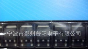
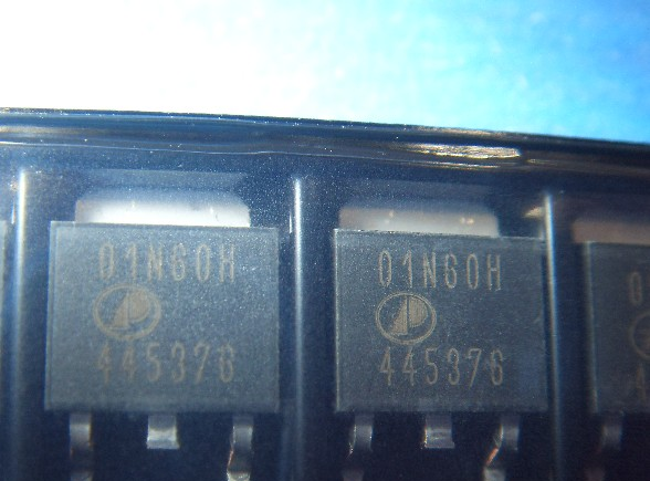
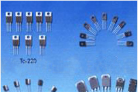
强势供应原装万代 AOD403
| 价 格: | 2.00 | |
| 品牌: | Alpha/阿尔法 | |
| 型号: | AOD403 | |
| 种类: | 绝缘栅(MOSFET) | |
| 沟道类型: | N沟道 | |
| 导电方式: | 增强型 | |
| 用途: | A/宽频带放大 | |
| 封装外形: | SMD(SO)/表面封装 | |
| 材料: | SIT静电感应 | |
| 开启电压: | 25(V) | |
| 夹断电压: | 25(V) | |
| 跨导: | 30(μS) | |
| 极间电容: | 20(pF) | |
| 低频噪声系数: | 10(dB) | |
| 漏极电流: | 20(mA) | |
| 耗散功率: | 100(mW) |
epetitive avalanche energy L=0.1mH C 120 mJ
Maximum Junction-to-Case C Steady-State °C/W
Thermal Characteristics
Parameter Units
Maximum Junction-to-Ambient A t ≤ 10s
RθJA
°C/W
°C/W
Absolute Maximum Ratings TA=25°C unless otherwise noted
V
±25 V
Pulsed Drain Current
Power Dissipation B
TC=25°C
Gate-Source Voltage
Drain-Source Voltage
Maximum Junction-to-Ambient A Steady-State
-85
-65
-200
Avalanche Current C -30
Power Dissipation A
TA=25°C
PDSM
Continuous Drain
Current B,G
Parameter Maximum Units
TA=25°C G
TA=100°C B
-30
W
Junction and Storage Temperature Range
A
PD
°C
100
50
-55 to 175
TC=100°C
ID
2.5
W
TA=70°C 1.6
AOD403
P-Channel Enhancement Mode Field Effect Transistor
Features
VDS (V) = -30V
ID = -85A (VGS = -20V)
RDS(ON) < 6mΩ (VGS = -20V)
RDS(ON) < 7.6mΩ (VGS = -10V)
General Description
The AOD403 uses advanced trench technology to
provide excellent RDS(ON), low gate charge and low
gate resistance. With the excellent thermal resistance
of the DPAK package, this device is well suited for
high current load applications. Standard Product
AOD403 is Pb-free (meets ROHS & Sony 259
specifications). AOD403L is a Green Product
ordering option. AOD403 and AOD403L are
electrically identical.
G D S
TO-252
D-PAK
Top View
Drain Connected
to Tab
G
D
S
Alpha & Omega Semiconductor, Ltd.
AOD403
Symbol Min Typ Max Units
BVDSS -30 V
-0.01 -1
TJ=55°C -5
IGSS ±100 nA
VGS(th) -1.5 -2.6 -3.5 V
ID(ON) -60 A
5.1 6
TJ=125°C 7.1 8.5
6.3 7.6 mΩ
gFS 44 S
VSD -0.72 -1 V
IS -104 A
Ciss 4360 5300 pF
Coss 1050 pF
Crss 762 pF
Rg 2.5 3 Ω
Qg 93.2 120 nC
Qgs 18 nC
Qgd 29.2 nC
tD(on) 18 25 ns
tr 30 45 ns
tD(off) 51 75 ns
tf 35 50 ns
trr 39.5 48 ns
Qrr 30.8 37 nC
THIS PRODUCT HAS BEEN DESIGNED AND QUALIFIED FOR THE CONSUMER MARKET. APPLICATIONS OR USES AS CRITICAL
COMPONENTS IN LIFE SUPPORT DEVICES OR SYSTEMS ARE NOT AUTHORIZED. AOS DOES NOT ASSUME ANY LIABILITY ARISING
OUT OF SUCH APPLICATIONS OR USES OF ITS PRODUCTS. AOS RESERVES THE RIGHT TO IMPROVE PRODUCT DESIGN,
FUNCTIONS AND RELIABILITY WITHOUT NOTICE.
Maximum Body-Diode Continuous Current
Input Capacitance
Output Capacitance
Turn-On DelayTime
DYNAMIC PARAMETERS
VGS=0V, VDS=-15V, f=1MHz
Gate Drain Charge
Turn-On Rise Time
Turn-Off DelayTime
VGS=-10V, VDS=-15V, RL=0.75Ω,
RGEN=3Ω
Gate resistance VGS=0V, VDS=0V, f=1MHz
Turn-Off Fall Time
SWITCHING PARAMETERS
Total Gate Charge
Gate Source Charge VGS=-10V, VDS=-15V, ID=-20A
mΩ
VGS=-10V, ID=-20A
IS=-1A,VGS=0V
VDS=-5V, ID=-20A
RDS(ON) Static Drain-Source On-Resistance
Forward Transconductance
Diode Forward Voltage
IDSS μA
Gate Threshold Voltage VDS=VGS ID=-250μA
VDS=-24V, VGS=0V
VDS=0V, VGS=±25V
Zero Gate Voltage Drain Current
Gate-Body leakage current
Electrical Characteristics (TJ=25°C unless otherwise noted)
STATIC PARAMETERS
Parameter Conditions
Body Diode Reverse Recovery Time
Body Diode Reverse Recovery Charge IF=-20A, dI/dt=100A/μs
Drain-Source Breakdown Voltage
On state drain current
ID=-250μA, VGS=0V
VGS=-10V, VDS=-5V
VGS=-20V, ID=-20A
Reverse Transfer Capacitance
IF=-20A, dI/dt=100A/μs
A: The value of R θJA is measured with the device mounted on 1in 2 FR-4 board with 2oz. Copper, in a still air environment with T A =25°C. The Power
dissipation PDSM is based on steady-state R θJA and the maximum allowed junction temperature of 150°C. The value in any given application depends
on the user's specific board design, and the maximum temperature of 175°C may be used if the PCB or heatsink allows it.
B. The power dissipation PD is based on TJ(MAX)=175°C, using junction-to-case thermal resistance, and is more useful in setting the upper dissipation
limit for cases where additional heatsinking is used. It is used to determine the current rating, when this rating falls below the package limit.
C: Repetitive rating, pulse width limited by junction temperature TJ(MAX)=175°C.
D. The R θJA is the sum of the thermal impedence from junction to case R θJC and case to ambient.
E. The static characteristics in Figures 1 to 6 are obtained using <300 μs pulses, duty cycle 0.5% max.
F. These tests are performed with the device mounted on 1 in 2 FR-4 board with 2oz. Copper, in a still air environment with T A=25°C. The SOA curve
provides a single pulse rating.
G. The maximum current rating is limited by the package current capability.
Rev 4: Aug 2005
Alpha & Omega Semiconductor, Ltd.
AOD403
TYPICAL ELECTRICAL AND THERMAL CHARACTERISTICS
-15
-12.8
THIS PRODUCT HAS BEEN DESIGNED AND QUALIFIED FOR THE CONSUMER MARKET. APPLICATIONS OR USES AS CRITICAL
COMPONENTS IN LIFE SUPPORT DEVICES OR SYSTEMS ARE NOT AUTHORIZED. AOS DOES NOT ASSUME ANY LIABILITY ARISING
OUT OF SUCH APPLICATIONS OR USES OF ITS PRODUCTS. AOS RESERVES THE RIGHT TO IMPROVE PRODUCT DESIGN,
FUNCTIONS AND RELIABILITY WITHOUT NOTICE.
0
20
40
60
80
100
0 1 2 3 4 5
-VDS (Volts)
Fig 1: On-Region Characteristics
-ID (A)
VGS=-2V
-4.5V
-5V
-6V
-10V
0
10
20
30
40
50
60
2 2.5 3 3.5 4 4.5 5
-VGS(Volts)
Figure 2: Transfer Characteristics
-ID(A)
0
2
4
6
8
10
0 10 20 30 40 50 60
-ID (A)
Figure 3: On-Resistance vs. Drain Current and Gate
Voltage
RDS(ON) (mΩ)
1.0E-06
1.0E-05
1.0E-04
1.0E-03
1.0E-02
1.0E-01
1.0E+00
1.0E+01
1.0E+02
0.0 0.2 0.4 0.6 0.8 1.0 1.2
-VSD (Volts)
Figure 6: Body-Diode Characteristics
-IS (A)
25°C
125°C
0.8
1
1.2
1.4
1.6
0 25 50 75 100 125 150 175
Temperature (°C)
Figure 4: On-Resistance vs. Junction Temperature
Normalized On-Resistance
VGS=-20V
VGS=-10V
4
8
12
16
20
24
4 8 12 16 20
-VGS (Volts)
Figure 5: On-Resistance vs. Gate-Source Voltage
RDS(ON) (mΩ)
25°C
125°C
VDS=-5V
VGS=-10V
ID=-20A
25°C
125°C
ID=-20A
VGS=-20V
-4V
Alpha & Omega Semiconductor, Ltd.
AOD403
TYPICAL ELECTRICAL AND THERMAL CHARACTERISTICS
-15
-12.8
THIS PRODUCT HAS BEEN DESIGNED AND QUALIFIED FOR THE CONSUMER MARKET. APPLICATIONS OR USES AS CRITICAL
COMPONENTS IN LIFE SUPPORT DEVICES OR SYSTEMS ARE NOT AUTHORIZED. AOS DOES NOT ASSUME ANY LIABILITY ARISING
OUT OF SUCH APPLICATIONS OR USES OF ITS PRODUCTS. AOS RESERVES THE RIGHT TO IMPROVE PRODUCT DESIGN,
FUNCTIONS AND RELIABILITY WITHOUT NOTICE.
0
2
4
6
8
10
0 10 20 30 40 50 60 70 80 90 100
-Qg (nC)
Figure 7: Gate-Charge Characteristics
-VGS (Volts)
0
1000
2000
3000
4000
5000
6000
7000
0 5 10 15 20 25 30
-VDS (Volts)
Figure 8: Capacitance Characteristics
Capacitance (pF)
Ciss
0
20
40
60
80
100
0.01 0.1 1 10 100 1000
Pulse Width (s)
Figure 10: Single Pulse Power Rating Junction-to-
Ambient (Note F)
Power (W)
0.001
0.01
0.1
1
10
0.00001 0.0001 0.001 0.01 0.1 1 10 100 1000
Pulse Width (s)
Figure 11: Normalized Maximum Transient Thermal Impedance (Note F)
ZθJA Normalized Transient
Thermal Resistance
Coss
Crss
0.1
1
10
100
1000
0.1 1 10 100
-VDS (Volts)
-ID (Amps)
Figure 9: Maximum Forward Biased Safe
Operating Area (Note F)
100μs
10ms
1ms
0.1s
1s
10s
DC
RDS(ON)
limited
TJ(Max)=150°C
TA=25°C
VDS=-15V
ID=-20A
Single Pulse
D=Ton/T
TJ,PK=TA+PDM.ZθJA.RθJA
RθJA=50°C/W
In descending order
D=0.5, 0.3, 0.1, 0.05, 0.02, 0.01, single pulse
TJ(Max)=150°C
TA=25°C
10μs
Ton
T
PD
Alpha & Omega Semiconductor, Ltd.
- 所属城市:浙江 宁波
- [联系时请说明来自维库仪器仪表网]
- 联系人: 奚圣建
- 电话:86 0574 87737972
- 传真:86 0574 87527478
- 手机:
- QQ :
长期供应开关三极管13001
信息内容:产品规格如下:3DD13001 TRANSISTOR (NPN)FEATURESpower switching applicationsMAXIMUM RATINGS (TA=25℃ unless otherwise noted)Symbol Parameter Value UnitsVCBO Collector -Base Voltage 600 VVCEO Collector-Emitter Voltage 400 VVEBO Emitter-Base Voltage 7 VIC Collector Current -Continuous 0.2 APC Collector Power Dissipation 0.75 WTJ Junction Temperature 150 ℃Tstg Storage Temperature -55-150 ℃
BTA08-600B可控硅
信息内容:dzsc/18/8735/18873525.jpg本公司现货供应BTA08-600B,品质优。
