供应HY5DU561622 256M(16M*16)DDR SDRAM内存芯片
| 价 格: | 面议 | |
| 型号/规格: | HY5DU561622ETP-4 | |
| 品牌/商标: | Hynix |
DDR SDRAM
是Double Data Rate Synchronous Dynamic Random Access Memory(双数据率同步动态随机存储器)的简称,是由VIA等公司为了与RDRAM相抗衡而提出的内存标准。DDR SDRAM是SDRAM的更新换代产品,采用2.5v工作电压,它允许在时钟脉冲的上升沿和下降沿传输数据,这样不需要提高时钟的频率就能加倍提高SDRAM的速度,并具有比SDRAM多一倍的传输速率和内存带宽,例如DDR 266与PC 133 SDRAM相比,工作频率同样是133MHz,但内存带宽达到了2.12 GB/s,比PC 133 SDRAM高一倍。目前主流的芯片组都支持DDR SDRAM,是目前最常用的内存类型。
DESCRIPTION描述
The Hynix HY5DU561622ETP is a 268,435,456-bit CMOS Double Data Rate(DDR) Synchronous DRAM, ideally suited
for the point-to-point applications which requires high bandwidth.
The Hynix 16Mx16 DDR SDRAMs offer fully synchronous operations referenced to both rising and falling edges of the
clock. While all addresses and control inputs are latched on the rising edges of the CK (falling edges of the /CK), Data,
Data strobes and Write data masks inputs are sampled on both rising and falling edges of it. The data paths are inter-
nally pipelined and 2-bit prefetched to achieve very high bandwidth. All input and output voltage levels are compatible
with SSTL_2.
FEATURES特性
• 2.5V +/-5% VDD and VDDQ power supply
supports 250/200 Mhz
• 2.6V +/- 0.1V VDD/VDDQ power supply supports
300/ 275Mhz
• 2.8V +/- 0.1V VDD/ VDDQ power supply supports
350Mhz
• All inputs and outputs are compatible with SSTL_2
interface
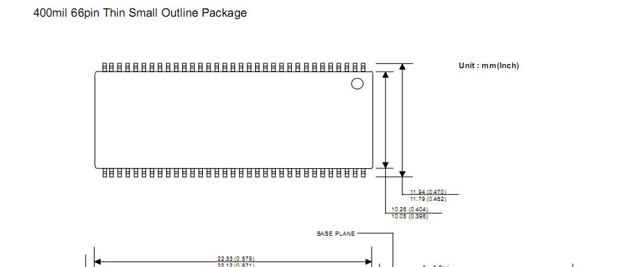
• JEDEC standard 400mil 66pin TSOP-II with 0.65mm
pin pitch
• Fully differential clock inputs (CK, /CK) operation
• Double data rate interface
• Source synchronous - data transaction aligned to
bidirectional data strobe (DQS)
• x16 device has 2 bytewide data strobes (LDQS,
UDQS) per each x8 I/O
• Data outputs on DQS edges when read (edged DQ)
Data inputs on DQS centers when write (centered
DQ)
• Data(DQ) and Write masks(DM) latched on the both
rising and falling edges of the data strobe
• All addresses and control inputs except Data, Data
strobes and Data masks latched on the rising edges
of the clock
• Write mask byte controls by LDM and UDM
• Programmable /CAS latency 3 / 4 / 5 supported
• Programmable Burst Length 2 / 4 / 8 with both
sequential and interleave mode
• Internal 4 bank operations with single pulsed /RAS
• tRAS Lock-Out function supported
• Auto refresh and self refresh supported
• 8192 refresh cycles / 64ms
产品糸列:
dzsc/18/2287/18228715.jpg
结构:
dzsc/18/2287/18228715.jpg
- 所属城市:广东 深圳
- [联系时请说明来自维库仪器仪表网]
- 联系人: 陈树辉
- 电话:0755-82534577/13076512089
- 传真:0755-82534577
- 手机:13686868407
- QQ :


供应汽车继电器/26.5*22*21/RD2-12
信息内容:dzsc/18/2287/18228716.gif RD Relays dzsc/18/2287/18228716.jpg Inrush current 100A 40A continuous rating at 70 ¡É PC Board terminal SPST & SPDT configurations Optional mounting bracke 1. Contact Data Contact Form 1A 1C Contact Material AgNi AgSnO Contact Ratings 1A:40A 14VDC 1C:30A 14VDC Max Switching Voltage 30VDC Max Switching Current 30A Max Switching Power 630W Contact Resistance 100m¥ØMax. at 6VDC 1A Life Expectancy Electrical 100,000 Operations (at30 Operations / minute) Machanical 10,000,000 Operations 2. General Data Insulation Resistance 100M Min at 500VDC Dielectric Strength Between Open Contacts 500VAC (for one minute) Between Contacts and coil 750VAC (for one minute) Operate Time 5ms Release Time 4ms Temperature Range -40 C to +85 C Shock Resistance 20G,11ms half sine wave pulse Vibration Resistanc...

供应HOLTEK稳压IC HT7550-1 SOT-89
信息内容:概述 HT75XX 系列是采用COMS 技术的三端口的低功耗高电压调整器允许输入电压可达24V 能输出从 3.0V-5.0V 的几个固定电压COMS 技术确保了低压降和低静态电流尽管检测器主要是设计成固定电压的 HT7550调整但通过外围元件也能获得可变的电压和电流 选择表1-1 型号 输出 电压允差 HT7530 3.0V +/-3% HT7533 3.3V +/-3% HT7536 3.6V +/-3% HT7544 4.4V +/-3% HT7550 5.0V +/-3% 上海联系电话:021-28716956,13681801778 深圳联系电话:13760171906 合泰电源管理芯片的详细介绍 HT7550简介HT7550-1是采用COMS技术的三端口低功耗高电压调整器。HT7550允许的输入电压可达24VHT7550特性 HT7550高输出电压精度HT7550精度±3% HT7550低输入输出电压差 HT7550典型值40mV HT7550低静态功耗电流 HT7550功耗范围(1.2-2.0)uA;典型值:1.5uA HT7550输出负载电流典型值: 100mA HT7550输出电压:5.0VHT7550高输入耐压24V HT7550低温度系数 HT7550-45-+85摄氏度 HT7550存储温度 -60-+120摄氏度 HT7550封装型式TO-92&SOT-89 HT75XX-1 -- 100mA Low Power LDO General Description The HT75XX-1 series is a set of three-terminal high current low voltage regulator imp...


